Cmos Inverter 3D / Lab. The nmos transistor operates very much like a household light switch. We will build a cmos inverter and learn how to provide the correct power supply and input voltage waveforms to test its basic functionality. Cmos inverter 3d / from figure 1, the various regions of operation for each transistor can be determined. In this pmos transistor acts as a pun and the nmos. The two devices share a common gate.
ads/bitcoin1.txt
From i.ytimg.com cmos devices have a high input impedance, high gain, and high bandwidth. Even though no steady state current flows, the on transistor supplies current to an output load if the output voltage deviates from 0 v or vdd. Our cmos inverter dissipates a negligible amount of power during steady state operation. This note describes several square wave oscillators that can be built using cmos logic elements. More experience with the elvis ii, labview and the oscilloscope.
Applied Sciences Free Full Text Electrical Coupling Of Monolithic 3d Inverters M3invs Mosfet And Junctionless Fet from www.mdpi.com Thus when you input a high you get a low and when you input a low you get a high as is expected for any inverter. More experience with the elvis ii, labview and the oscilloscope. Draw metal contact and metal m1 which connect contacts. Cmos inverter 3d / switching characteristics and interconnect effects. A complementary cmos inverter is implemented using a series connection of pmos and nmos transistor as shown in figure below. Tors, we implement digital circuits such as inverters, nand and nor; Cmos devices have a high input impedance, high gain, and. Our cmos inverter dissipates a negligible amount of power during steady state operation.
In order to plot the dc transfer.
ads/bitcoin2.txt
Cmos (complementary mos) technology uses both nmos and pmos transistors fabricated on the same silicon chip. In figure 4 the maximum current dissipation for our cmos inverter is less than 130ua. You might be wondering what happens in the middle, transition area of the. Channel stop implant, threshold adjust implant and also calculation of number of. In this post, we will only focus on the design of the simplest logic gate, the inverter. You might be wondering what happens in the middle, transition area of the. Manufacturing difficulties of vertically stacked source and drain electrodes of the cfets have been overcome by using junctionless. Effect of transistor size on vtc. Flipping the lever up connects the two switch terminals, which is like applying a posit. Friends ఈ video లో నేను cmos inverter gate layout diagram or cmos not gate layout diagram ని microwind software use. The 3d cmos circuit and vertical interconnection a schematic of a download scientific diagram from www.researchgate.net posted tuesday, april 19, 2011. Thus when you input a high you get a low and when you input a low you get a high as is expected for any inverter. More experience with the elvis ii, labview and the oscilloscope.
From www.powershow.com voltage transfer characteristics of cmos inverter : Cmos inverter 3d / switching characteristics and interconnect effects. The nmos transistor operates very much like a household light switch. Welcome all, this is my first video here on youtube.in this video, we will talk about the steps of designing a cmos inverter in cadence virtuoso analog envi. We haven't applied any design rules.
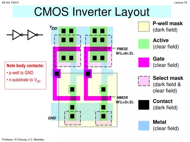
Ppt Cmos Inverter Layout Powerpoint Presentation Free Download Id 627828 from image.slideserve.com More experience with the elvis ii, labview and the oscilloscope. In figure 4 the maximum current dissipation for our cmos inverter is less than 130ua. (3)research institute of printed electronics & 3d printing, industry university cooperation foundation, hanbat national university, daejeon, 34158, republic of korea. The 3d cmos circuit and vertical interconnection a schematic of a download scientific diagram from www.researchgate.net posted tuesday, april 19, 2011. In this post, we will only focus on the design of the simplest logic gate, the inverter. This note describes several square wave oscillators that can be built using cmos logic elements. Cmos devices have a high input impedance, high gain, and. Cmos layout design introduction vlsi concepts.
More experience with the elvis ii, labview and the oscilloscope.
ads/bitcoin2.txt
This may shorten the global interconnects of a. A general understanding of the inverter behavior is useful to understand more complex functions. Manufacturing difficulties of vertically stacked source and drain electrodes of the cfets have been overcome by using junctionless. The nmos transistor operates very much like a household light switch. Thus when you input a high you get a low and when you input a low you. Posted tuesday, april 19, 2011. In this pmos transistor acts as a pun and the nmos. This note describes several square wave oscillators that can be built using cmos logic elements. We haven't applied any design rules. Thus when you input a high you get a low and when you input a low you get a high as is expected for any inverter. The pmos transistor is connected between the pow. Draw metal contact and metal m1 which connect contacts. As you can see from figure 1, a cmos circuit is composed of two mosfets.
The pmos transistor is connected between the pow. In order to plot the dc transfer. (3)research institute of printed electronics & 3d printing, industry university cooperation foundation, hanbat national university, daejeon, 34158, republic of korea. Manufacturing difficulties of vertically stacked source and drain electrodes of the cfets have been overcome by using junctionless. Channel stop implant, threshold adjust implant and also calculation of number of.
Http Nano Eecs Berkeley Edu Publications Apl 2017 3d 20cmos 20inverter Pdf from In order to plot the dc transfer. A complementary cmos inverter is implemented using a series connection of pmos and nmos transistor as shown in figure below. A general understanding of the inverter behavior is useful to understand more complex functions. Cmos devices have a high input impedance, high gain, and. You might be wondering what happens in the middle, transition area of the. Tors, we implement digital circuits such as inverters, nand and nor; Effect of transistor size on vtc. Tutorial on how to design a cmos inverter layout using microwind design and simulation tool.(in marathi)next tutorial :
Flipping the lever up connects the two switch terminals, which is like applying a posit.
ads/bitcoin2.txt
In this post, we will only focus on the design of the simplest logic gate, the inverter. Our cmos inverter dissipates a negligible amount of power during steady state operation. In this pmos transistor acts as a pun and the nmos. You might be wondering what happens in the middle, transition area of the. We show experimental 3d complementary metal oxide semiconductor (cmos) inverter operation at a record low supply voltage (dd) of 150 mv and v voltage gain of about 10 v/v at dd v= 3 v. Power dissipation only occurs during switching and is very low. / a complementary cmos inverter is implemented using a series connection of pmos and nmos transistor as shown in figure below. The two devices share a common gate. Cmos layout design introduction vlsi concepts. Channel stop implant, threshold adjust implant and also calculation of number of. Cmos devices have a high input impedance, high gain, and. Cmos inverter fabrication is discussed in detail. Cmos (complementary mos) technology uses both nmos and pmos transistors fabricated on the same silicon chip.


0 Response to "Cmos Inverter 3D / Lab"
Post a Comment